
- de
- en

How can a specific range of functions be integrated into the circuit board?
Vertical integration is opening up new horizons in the design of electronic modules. That's because circuit carriers with embedded electronic components are capable of much more than merely securing components and connecting these together conductively. The uncramping of space-critical layouts, improved heat dissipation, more favourable HF characteristics or the possibility of a system integration are just some of the advantages that can be achieved with device embedded substrates.
KSG Leiterplatten GmbH confronts the demands of its customers in terms of new functional units by utilising different embedding techniques. In several R&D projects, the technological principles of different embedding approaches are currently being examined. At the same time the company is playing a part in the DKE working group aligned with this research in order to develop appropriate Standards.
KSG is presently focusing their activities on the structure and/or integration of passive electronic elements [embedded components], on the implementation of identification tags [embedded RFID] as well as the realisation of ultra-flat display elements [embedded display] by utilising the most divers embedding techniques. Based on selected examples, the following is to describe the practical implementation.
It is vitally important here that intercommunication takes place between the designer and the circuit board manufacturer at the earliest possible point in the product development process. Let us together implement the advantages of this structure, connection and encapusulating technique in your product ideas!
Embedded RFID
|
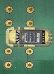
An important focus of research for KSG is the integration of identification tags. The information lodged on the chip can be read contactlessly and supplemented by further data. Retraceability and protection against plagiarism are two reasons why RFID tags are not placed on the surface of the circuit board but are embedded inside a multilayer circuit substrate. Implementation of the tag also necessitates the incorporation of active electronic components into the layer structure. |
|
| IC and antenna are conceived for the UHF band (868 MHz). The antenna size and its design depends on the respective application. Even with a minimal tag area of approx. 1 cm a reading distance of more than 1 cm² can be achieved with moderate reader transmission power. The antenna can be incorporated into the conductive pattern from the inner or outer layer. Complete freedom of the coil or dipole shaped antenna structures from tangential conductive pattern areas on the same level or above or below is often not necessary. A cavity must be reserved for the RFID chip prior to the pressing. |
Circuit board with implemented RFID tags |
Embedded components
|
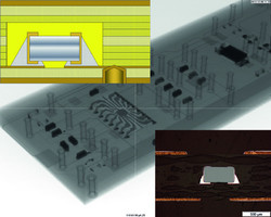
Resistors, condensers and inductances can nowadays be integrated into the circuit board internals as discrete elements. By means of conventional structuring and connection technologies such as soldering or conductive gluing these are contacted on an inner layer or secured in cavities and tethered directly by means of vias. Fig. 1 shows a “buried” SMD resistor. In the circuit board composite, embedded condensers exhibit advantages which shouldn't be underestimated. |
Circuit board section with integrated resistor |
Compared to their surface mountable counterparts, the parasitic inductances are significantly lower, the condensers can be brought spatially closer to the IC connections and it is to some extent possible to replace several discrete capacitive elements with a single integrated condenser.
Alternatively, passive elements can also be built up additively on inner layers and where applicable be structured using conventional subtractive techniques. The layer structure can be effected by means of screen or ink-jet printing or equally by means of introducing further specific functional layers such as thin laminates into the layer stack or “book”. For selected electronic components such as planar coils only a selective removal is necessary under certain circumstances.
Technologies for structuring or embedding passive electronic components have been and are being investigated in several R&D projects. In this regard KSG works jointly with well-known partners from industry and research.
Focus of research and development activities
Integration of functionalities in the circuit board
Vertical integration is opening up new horizons in the design of electronic modules. That is because circuit carriers with embedded electronic components are capable of much more than merely securing components and connecting these together conductively.
The gain in area for the securing of components, improved heat dissi- pation, more economical HF characteristics or the possibility of system integration are just a few of the advantages that can be achieved with device embedded substrates.
KSG is currently focusing its activities on the integration of passive and active components (embedded components) in three integration technologies.
Cavity technology
Production of cavities by means of mechanical depth milling or a combination of mechanical depth milling and laser removal.
Embedded switch (MEMS)
<p><img id="itool-image-1109" src="files/PHPSESSID/ocbgcd7vfjap36p5b8b5kssl25/1493127707/0/0/1/1109.jpg" alt="Eingebetteter Inertialsensor (MEMS)" width="267" height="250" /></p>
Embedded inertial sensor (MEMS) and ASIC
"Embedding" of passive /active components by pressing a component-populated inner layer in the multilayer composite by means of:
Pad bonding technology
Press bonding a component-populated and soldered inner layer. The electrical contact is made by soldering. An interconnection of the component connections is necessary.
Via connection technology
Press bonding a component-populated and soldered inner layer. The electrical contact is made by means of metallised laser vias directly onto the component connections. An interconnection can thereby be dispensed with.
Resistors, capacitors and inductances can nowadays be integrated into the circuit board interior as discrete components. By means of conventional structuring and connection technologies such as soldering or conductive gluing these are contacted on an inner layer or secured in cavities and tethered directly by means of vias.
In the circuit board composite, embedded capacitors (see Fig.) exhibit many advantages. In comparison to their surface mountable pendants, the parasitic inductances are significantly less and the capacitors can be brought spatially closer to the IC connections.
Further advantages of these technologies:
- Substitute for board-to-board assemblies
- Assembly miniaturisation
- Touch protection
- Housing substitute
- Piracy protection
- Improved heat management
- EMC protection (Faraday cage)
- Protection against environmental influences (air humidity, pressure, vibration, impact etc.)