
- de
- en
Experts in circuit boards

Layer structure
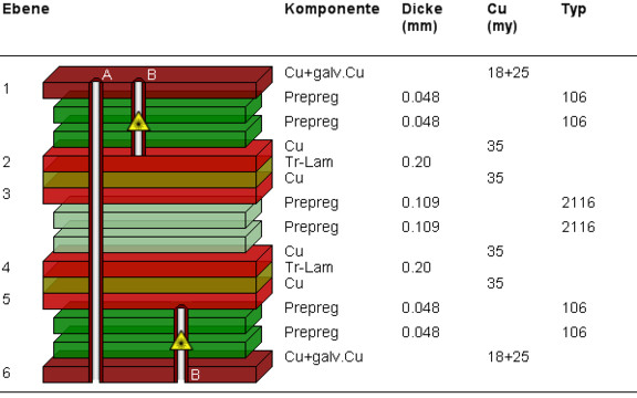
| Pressed board thickness * | 0.97 +/- 10% |
| Overall thickness incl. galv. Cu and solder resist mask * | 1.08 +/- 10% |
Notes on layer structure:
- * Thickness calculation with unfilled FR-4 base material at 50% copper allocation on the inner layers (depending on base material type, selected copper thickness and copper allocation, deviating resultant insulation and end thicknesses)
- Thickness tolerance of base material +/-10%
- Minimum copper end thicknesses in accordance with IPC 6012, current edition
Design rules for layer structuring
| Through-holes [A] (vias) |
End Ø Via pad Ø |
≥ 150 µm ≥ 450 µm |
| Laser blind holes [B] (blind vias) |
End Ø Via pad Ø |
≥ 100 µm ≥ 350 µm |
| Conductive pattern, outer layers |
||
| Conductor width with 9 µm copper base Conductor spacing with 9 µm copper base |
≥ 80 µm ≥ 100 µm |
|
| Standard |
Conductor width with 18 µm copper base Conductor spacing with 18 µm copper base |
≥ 100 µm ≥ 120 µm |
| Conductive pattern, inner layers | ||
| Conductor width with 18 µm copper base Conductor spacing with 18 µm copper base |
≥ 65 µm ≥ 80 µm |
|
| Standard |
Conductor width with 35 µm copper base Conductor spacing with 35 µm copper base |
≥ 85 µm ≥ 100 µm |